T.O AN 16-40BC348-3
HANDBOOK
MAINTENANCE INSTRUCTIONS
RADIO RECEIVERS
BC-348-J BC-348-N BC-348-Q
THIS PUBLICATION REPLACES T.O. AN-08-10-112 DATED 18 DECEMBER 1943
PUBLISHED UNDER AUTHORITY OF THE SECRETARY OF THE AIR FORCE
REVISED 21 JUNE1948
OCR by Bill, NJ7P
From a partial Manual from
Fair Radio Sales
This manual is missing the comprehensive parts lists and some of the pictures from the original manual. The full text and key data is present.TABLE OF CONTENTS
I. GENERAL DESCRIPTIONHandbook of
MAINTENANCE INSTRUCTIONS
For
RADIO RECEIVERS
BC-348-J, BC-348-N and BC-348-Q
SPECIAL NOTICE
Radio Receivers BC-348-J, BC-348-N and BC-348-Q are essentially alike. Therefore, reference will be made throughout the book to these receivers as follows: Radio Receiver BC-348-(*). However, all photographs and diagrams will be labeled for the "J" equipment, since it applies equally well to the other two models.|
Description |
Size in Inches |
Weight in Pounds |
|
1 Radio Receiver BC-348-(*) Complete (Includes Dynamotor DM-28-(*) and Mounting FT-I54-J, FT-154-Q or FT-154-AA) |
18 x 10 1/2 x 9 1/2 high |
38.0 |
|
1 Mounting FT-I54-J, FT-I54-Q or FT-154-AA (Does not include Plug PL-P103 or PL-Q103) |
18 x 8 1/2 x 1 3/8 high |
3.843 |
|
1 Plug PL-P103 or Plug PL-Q103 |
l 5/s x 2 1/8 x 2 7/8 high 2 x 2 1/8 x 3 high |
.312 .375 |
|
1 Set of 8 Vacuum Tubes, 2 Pilot Lights, 1 Fuse |
.563 |
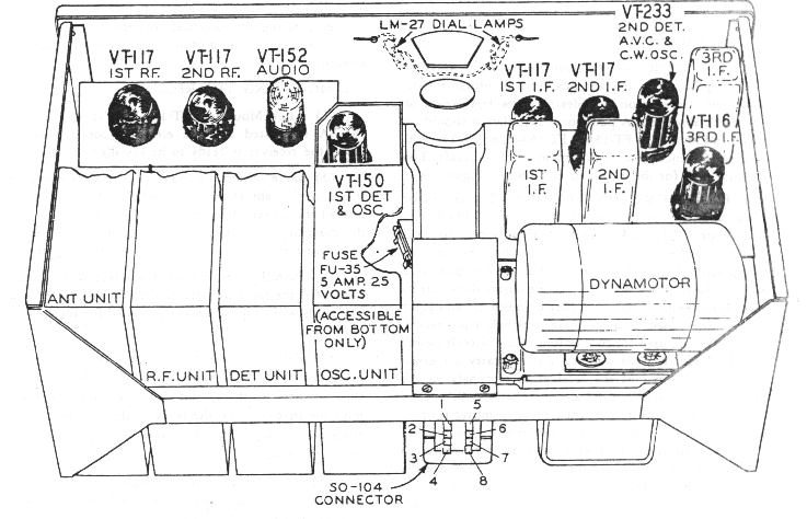
Figure 2 – Radio receiver BC-348-J, Tube Positions
(10) Loosen the thumbscrews in the lower part of the handles on the front panel and pull the chassis from the cabinet.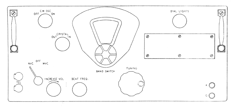
Figure 3 – Radio Receiver BC-348-J, View of front Panel
b. CONTROLS.NOTE
All tuning should be done on MVC switch with the volume control advanced only enough to give the desired signal strength. In the absence of a signal the setting of the volume control can be judged by the loudness of the background noise. On MVC with the volume control set at maximum, very strong carrier waves will block the receiver and intelligible signals cannot be received.NOTE
Tuning should be done in the MVC position with the volume control advanced only as far as required for a comfortable output level. While waiting for the tubes to warm up, adjust the dial light control for the desired dial illumination and turn the band switch to the frequency band in which the signals to be received are transmitted.NOTE
The crystal band pass filter is intended primarily for use in c-w reception. However, the added selectivity may at times prove helpful in receiving modulated signals through heavy interference.|
Band |
Frequency Range |
|
1 |
200 -- 500 Kilocycles |
|
2 |
1.5- 3.5 Megacycles |
|
3 |
3.5 ~ 6.0 Megacycles |
|
4 |
6.0 ~ 9.5 Megacycles |
|
5 |
9.5--13.5 Megacycles |
|
6 |
13.5--18.0 Megacycles |
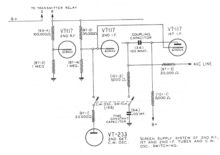
Figure 4 – C-W Oscillator Switching
The effects of ambient temperature variations are minimized by the use of a temperature compensated tuned circuit. The c-w oscillator operates at an extremely low level, minimizing harmonics and stray oscillator pickup. The output is capacitively coupled to the plate circuit of the second amplifier tube by a twisted wire capacitor. Amplification by the third i-f amplifier stage, the gain of which is not controlled either manually or by a-v-c, provides sufficient output from the c-w oscillator to the diode detector. This value of oscillator output is somewhat below the level at which the a-v-c operates, thus permitting the use of automatic volume control even for c-w reception.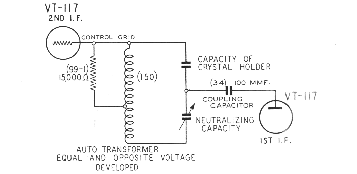
Figure 5 – Crystal Filter Circuit
25. SECOND DETECTOR.TABLE A – CHARACTERISTICS OF TUBES, LAMPS AND FUSE
TUBE CHARACTERISTICS
|
Tube Type |
RMA Equivalent |
Heater Volts/Amps |
Plate Volts |
Screen Volts |
Grid Volts |
Plate Ma. |
Screen Ma. |
Mu |
Plate Resistance |
Transconductance Micromhos |
|
VT-116 |
6SJ7 |
6.3/0.3 |
250 |
100 |
-3.0 |
3.0 |
0.8 |
2500 |
1,500,000 |
1650 |
|
VT-117 |
6SK7 |
6.3/0.3 |
250 |
100 |
-3.0 |
9.2 |
2.4 |
1600 |
800,000 |
2000 |
|
VT-150 |
6SA7 |
6.3/0.3 |
250 |
100 |
-2.0 |
3.4 |
8.0 |
800,000 |
||
|
VT-162 |
6K6 |
6.3/0.4 |
250 |
250 |
-18.0 |
32.0 |
5.5 |
150 |
68,000 |
2200 |
|
VT-233 |
6SR7 |
6.3/0.3 |
250 |
-9.9 |
9.5 |
16 |
8,500 |
1900 |
DIAL LAMPS
|
Type |
RMA Equivalent |
Volts |
Amps. |
|
LM-27 |
No. 44 |
6.3 |
0.25 |
FUSE
|
Type |
Volts |
Amps. |
|
FU-35 |
25 |
5.0 |
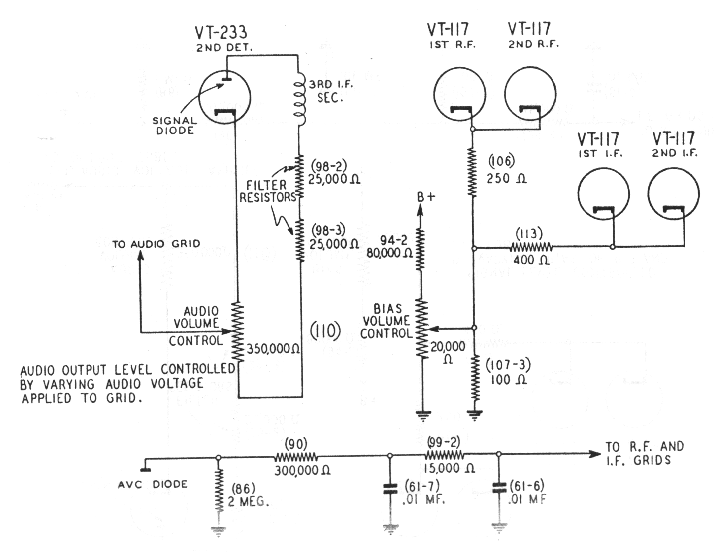
Figure 6 – AVC Connections
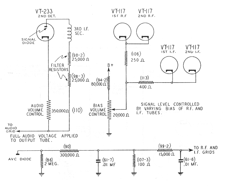
Figure 7 – MVC Connections
V. MAINTENANCENOTE
A standard signal generator, a phantom antenna, a Test Set 1-56-A and other like equipment should be used when servicing and aligning Radio Receiver BC-348-(*)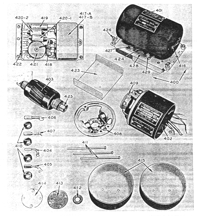
Figure 8 – Dynamotor, DM-28 (*)
c. COMMUTATORNOTE
The bearing support bracket is more readily removable from the frame by a slight tilting back and forth of the frame with respect to the bracket.|
INPUT |
OUTPUT |
||
|
Volts |
Amperes |
Volts |
Amperes |
|
24 |
0.7 |
215 |
0. |
|
24 |
1.1 |
210 |
30. |
|
24 |
1.3 |
202 |
60. |
|
28 |
0.8 |
258 |
0. |
|
28 |
1.1 |
246 |
40. |
|
28 |
1.5 |
236 |
75. |
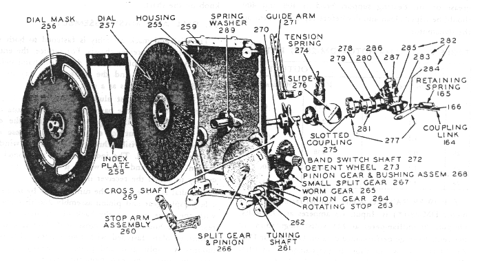
Figure 9 – Radio Receiver BC-348-J, Dial and Mask Assembly
e. REPLACEMENT OF DIAL AND MASK ASSEMBLY.NOTE
All tubes of a given type supplied with the equipment shall be consumed prior to employment of tubes from general stock.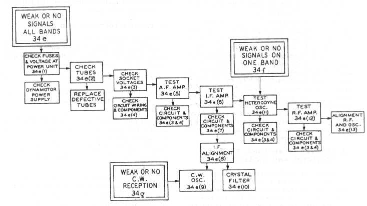
Figure 10 – Trouble Location and Correction Chart
c. TROUBLE LOCATION AND CORRECTION PROCEDURE.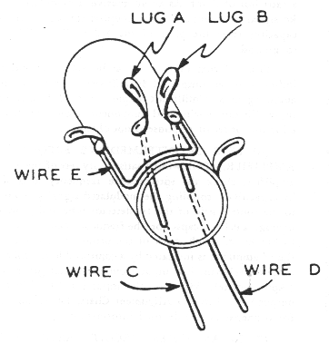
Figure 11 – Crystal Filter Coil
(10) NEUTRALIZING THE CRYSTAL CIRCUIT.--AII crystal circuits are properly neutralized at the factory before being shipped. Ordinarily, reneutralizing is not required unless the neutralizing coil and capacitor (Ref. 150) or crystal and switch assembly (Ref. 160 and 167) have been replaced, or unless the crystal circuit appears to be excessively broad. If neutralizing is necessary it may be done as follows:NOTE
When making measurements at the second r-f tube, the flexible lead on the orange adapter plug must be removed from the pin jack marked GND and inserted in the outer No. 3 jack, as the shield is not grounded.TABLE C -- TUBE SOCKET VOLTAGE CHART
THE VOLTAGES ARE READ BETWEEN THE SOCKET TERMINAL AND GROUND UNDER THE|
Socket, terminal or Block No. |
6SK7 VT-117 1st R-F |
6SK7 VT-117 2st R-F |
6SA7 VT-150 1st Det. |
6SK7 VT-117 1st I-F |
6SK7 VT-117 2nd I-F |
6SJ7 VT-116 3rd I-F |
6SR7 VT-233 2nd Det. C-W Osc. |
6K6 VT-152 Audio |
|
1. |
Shell 0 V. |
Shell 8 V. Note A |
Shell 0 V. |
Shell 0 V. |
Shell 0 V. |
Shell 0 V. |
Shell 0 V. |
0 V. |
|
2. |
Heater 18.9 V |
Heater 12.6 V. |
Heater 0 V. |
Heater 25.2 V. |
Heater 12.6 V. |
Heater 6.3 V. |
Grid 6 V. Note D |
Heater 25.3 V. |
|
3. |
Sup 0 V. |
Sup. 3.8 V. |
Plate 210 V. 2 Ma. |
Sup. 5.8 V. |
Sup. 5.8 V. |
Sup. 16.5 V. |
Cathode 16.5 V |
Plate 200 V. 18 Ma. |
|
4. |
Grid 0 V. |
Grid 0 V. |
Screen 100 V. Note C 6.2 Ma. |
Grid 0 V. |
Grid 0 V. |
Grid 14 V. |
Diode 2 V. |
Screen 210 V. 3.4 Ma. |
|
5. |
Cathode 3.8 V. |
Cathode 3.8 V. |
Osc Grid -.4 V |
Cathode 5.8 V. |
Cathode 5.8 V. |
Cathode 16.5 V. |
Diode 0 V. |
Grid -8 V. Note E |
|
6. |
Screen 100 V. 2 Ma. |
Screen 83 V. 1.6 Ma. |
Cathode 0 V. |
Screen 105 V. 1.6 Ma. |
Screen 105 V. 1.6 Ma. |
Screen 100 V. .85 Ma. |
Plate 55 V. Note B (C-W Osc. ON) .95 Ma |
Tie Terminal .2 V. |
|
7. |
Heater 12.6 V |
Heater 6.3 V |
Heater 6.3 V |
Heater 18.9 V |
Heater 18.9 V |
Heater 0 V |
Heater 6.3 V |
Heater 18.9 V |
|
8. |
Plate 100 V. 9 Ma. |
Plate 170 V. 6 Ma. |
Grid -1.8 V. |
Plate 185 V. 5.4 Ma. |
Plate 210 V. 5.8 Ma. |
Plate 210 V. 3.5 Ma. NOTE F |
Heater 12.6 V. |
Cathode 0 V. |
TABLE D -- RESISTANCES BETWEEN SOCKET TERMINALS AND GROUND
RESISTANCE READINGS ARE MADE UNDER THE FOLLOWING CONDITIONS:|
Socket, terminal or Block No. |
6SK7 VT-117 1st R-F |
6SK7 VT-117 2st R-F |
6SA7 VT-150 1st Det. |
6SK7 VT-117 1st I-F |
6SK7 VT-117 2nd I-F |
6SJ7 VT-116 3rd I-F |
6SR7 VT-233 2nd Det. C-W Osc. |
6K6 VT-152 Audio |
|
1. |
Shell 0. |
Shell 250 Note A |
Shell 0 |
Shell 0 |
Shell 0 |
Shell 0 |
Shell 0 |
0 |
|
2. |
Heater 6.5 |
Heater 5.5. |
Heater 0 |
Heater 6.5. |
Heater 5.5. |
Heater 3. |
Grid 100,000 |
Heater 6.5 |
|
3. |
Sup 0 |
Sup. 250 |
Plate 520 |
Sup. 420 |
Sup. 420 |
Sup. 4000 |
Cathode 4000 |
Plate 1200 |
|
4. |
Grid 1 Meg AVC 3.3 Meg |
Grid 90,000 AVC 2.4 Meg |
Screen 20,000 |
Grid 15,000 AVC 2.3 Meg |
Grid 15,000 AVC 2.3 Meg. |
Grid 3500 |
Diode 400,000 |
Screen 900. |
|
5. |
Cathode 250 |
Cathode 250 |
Osc 80,000 |
Cathode 420 |
Cathode 420 |
Cathode 4000 |
Diode 260,000 AVC 2 Meg |
Grid 1.1 Meg |
|
6. |
Screen 15,000 |
Screen 500,000 |
Cathode 1.2 |
Screen 500,000 |
Screen 500,000 |
Screen 120,000. |
Plate 500,000 5 Meg Osc ON |
Tie Terminal .5 |
|
7. |
Heater 5.5 |
Heater 4 |
Heater 4 |
Heater 6.5 |
Heater 6.5 |
Heater 0 |
Heater 3 |
Heater 6.5 |
|
8. |
Plate 15,000 |
Plate 10,000 |
Grid 1 Meg |
Plate 5500 |
Plate 500 |
Plate 1500 |
Heater 5.5 |
Cathode 0 |
TABLE E -- ADDITIONAL POINTS TO MAKE CONTINUITY
RESISTANCE READINGS TO GROUND
RESISTANCE READINGS MADE UNDER THE SAME CONDITIONS|
POWER CONNECTOR (175) |
OUTPUT TRANSFORMER And CHOKE (155-A and B) |
DYNAMOTOR TERMINAL STRIP |
||
|
Terminal Numbers On Connector |
Resistance |
Terminal Numbers On Unit |
Resistance |
Readings from low Voltage to High Voltage end |
|
1. |
150 ohms |
1. |
16 ohms |
0 |
|
2. |
500 ohms |
2. |
150 ohms |
1.5 ohms Note A |
|
3. |
1.5 ohms Note A |
3. |
500 ohms |
1.5 ohms Note A |
|
4. |
1.5 ohms Note A |
4. |
1200 ohms |
270 ohms |
|
5. |
0 |
5. |
25 ohms |
500 ohms |
|
6. |
500,000 ohms |
6. |
270 ohms |
|
|
7. |
0 |
|||
|
8. |
0 |
|||
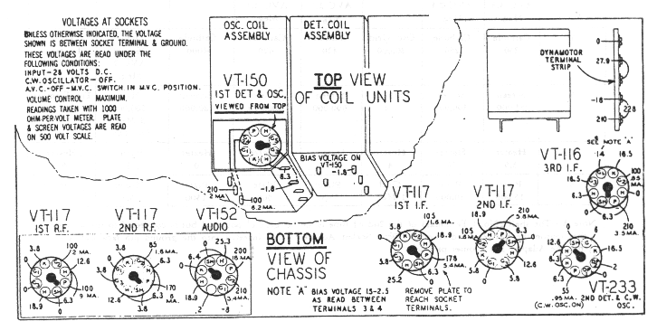
Figure 12 – Socket Voltages
TABLE F -- COIL CHARACTERISTICS
Inductance Readings Given in Microhenries. All D.C. Resistance Readings Given in Ohms. Inductance Measurements Made at 1,000 Cycles. Resistance Readings Within +/-10%. With Coil Removed from Shield. "Q" Readings Made With Coil Removed From Shield. Primary Inductance Readings Within +/-5%. "Q" Readings Within +/-20%. Secondary Inductance Readings Within +/-2%..|
Band No. |
Coil Ref. No. |
Inductance |
D.C. Resistance |
Q |
Frequency for "Q" Measurement |
|||
|
Pri. |
Sec. |
Pri. |
Sec. |
Pri. |
Sec. |
|||
|
ANTENNA UNIT |
||||||||
|
1 |
120 |
1348.7 |
1864.7 |
125 |
16.5 |
88 |
500 KC(5) |
|
|
2 |
121 |
298.7 |
27.8 |
13.8 |
0.75 |
145 |
1.5 MC(5) |
|
|
3 |
122 |
39.0 |
4.6 |
4.5 |
0.18 |
122 |
6.0 MC(5) |
|
|
4 |
123 |
14.5 |
1.1 |
3.0 |
0.11 |
157 |
9.5 MC(5) |
|
|
5 |
124 |
10.2 |
0.6 |
2.4 |
0.03 |
139 |
13.5 MC(5) |
|
|
6 |
125 |
3.0 |
0.1 |
1.4 |
0.02 |
173 |
18.0 MC(5) |
|
|
Band No. |
Coil Ref. No. |
Inductance |
D.C. Resistance |
Q |
Frequency for "Q" Measurement |
|||
|
Pri. |
Sec. |
Pri. |
Sec. |
Pri. |
Sec. |
|||
|
R-F UNIT |
||||||||
|
1 |
126 |
(7) |
2439.7 |
|
61.5 |
74 |
500 KC(5) |
|
|
2 |
127 |
(7) |
41.6 |
0.49 |
3.1 |
99 |
1.5 MC(5) |
|
|
3 |
128 |
(7) |
7.0 |
0.53 |
0.2 |
161 |
6.0 MC(5) |
|
|
4 |
129 |
(7) |
2.0 |
0.52 |
0.1 |
162 |
9.5 MC(5) |
|
|
5 |
130 |
(7) |
1.2 |
0.52 |
0.04 |
217 |
13.5 MC(5) |
|
|
6 |
131 |
(7) |
0.3 |
0.75 |
0.03 |
220 |
18.0 MC(5) |
|
|
Band No. |
Coil Ref. No. |
Inductance |
D.C. Resistance |
Q |
Frequency for "Q" Measurement |
|||
|
Pri. |
Sec. |
Pri. |
Sec. |
Pri. |
Sec. |
|||
|
DETECTOR UNIT |
||||||||
|
1 |
132 |
(7) |
2433.7 |
|
61.5 |
74 |
500 KC(5) |
|
|
2 |
133 |
(7) |
41.6 |
0.49 |
3.1 |
99 |
1.5 MC(5) |
|
|
3 |
134 |
(7) |
7.0 |
0.53 |
0.2 |
161 |
6.0 MC(5) |
|
|
4 |
135 |
(7) |
2.0 |
0.52 |
0.1 |
162 |
9.5 MC(5) |
|
|
5 |
136 |
(7) |
1.2 |
0.52 |
0.04 |
217 |
13.5 MC(5) |
|
|
6 |
137 |
(7) |
0.3 |
0.75 |
0.03 |
220 |
18.0 MC(5) |
|
|
Band No. |
Coil Ref. No. |
Inductance |
D.C. Resistance |
Q |
Frequency for "Q" Measurement |
|||
|
Pri. |
Sec. |
Pri. |
Sec. |
Pri. |
Sec. |
|||
|
OSCILLATOR UNIT |
||||||||
|
1 |
138 |
(7) |
346.9 |
1.2 |
6.3 |
96 |
1.0 MC |
|
|
2 |
139 |
(7) |
25.8 |
0.7 |
1.1 |
152 |
12.5 MC |
|
|
3 |
140 |
(7) |
5.3 |
0.54 |
0.24 |
114 |
7.0 MC |
|
|
4 |
141 |
(7) |
1.6 |
0.9 |
0.07 |
156 |
10.5 MC |
|
|
5 |
142 |
(7) |
1.5 |
0.4 |
0.06 |
160 |
12.5 MC |
|
|
6 |
143 |
(7) |
0.4 |
0.76 |
0.03 |
179 |
17.0 MC |
|
|
Band No. |
Coil Ref. No. |
Inductance |
D.C. Resistance |
Q |
Frequency for "Q" Measurement |
|||
|
Pri. |
Sec. |
Pri. |
Sec. |
Pri. |
Sec. |
|||
|
I-F COILS |
||||||||
|
1st I-F |
147 |
120(1) |
120(1) |
1.5(2) |
1.5(2) |
129 |
128 |
915 KC(3) |
|
2nd I-F |
148 |
120(1) |
120(1) |
1.5(2) |
1.5(2) |
129 |
128 |
915 KC(3) |
|
3rd I-F |
149 |
120(1) |
242(1) |
1.5(2) |
5.0(2) |
128 |
112 |
915 KC(3) |
|
Band No. |
Coil Ref. No. |
Inductance |
D.C. Resistance |
Q |
Frequency for "Q" Measurement |
|||
|
Pri. |
Sec. |
Pri. |
Sec. |
Pri. |
Sec. |
|||
|
MISCELLANEOUS COILS |
||||||||
|
Xtal Neut |
150 |
|
2.03 |
52.75 |
56(6) |
400 KC |
||
|
C-W Osc. |
151 |
1.9(1) |
125.5(1) |
0.21(2) |
1.74(2) |
77 |
915 KC(3) |
|
|
I-F Trap |
152 |
|
60.9 |
|
2.3 |
74 |
915 KC |
|
|
Choke |
420 |
|
466.2(4) |
|
12.0 |
|
|
|
|
Choke |
421 |
|
79.1(4) |
|
0.15 |
|
|
|
TABLE G -- ALIGNMENT CHART
|
RECEIVER CONTROLS |
3rd I.F. |
2nd I.F. |
1st I.F. |
No. 1 Band |
|
|
C.W. Osc. |
OFF |
OFF |
OFF |
OFF |
|
|
Crystal |
OUT |
OUT |
OUT |
OUT |
|
|
AVC-OFF-MVC |
MVC |
MVC |
MVC |
MVC |
|
|
Volume |
Maximum |
Maximum |
Maximum |
Maximum |
|
|
Band Sw. Setting |
No. 2 Band 1.5-3.5 Mc |
No. 2 Band 1.5-3.5 Mc |
No. 2 Band 1.5-3.5 Mc |
No. 1 Band 200-500 kc |
|
|
Tuning Control Position |
1.5 Mc |
1.5 Mc |
1.5 Mc |
470 kc |
|
|
SIGNAL GENERATOR |
Antenna Connections |
3rd I.F. Tube VT-116 Control Grid Socket Terminal No. 4 |
2nd I.F. Tube VT-117 Control Grid Socket Terminal No. 4 |
1st Det. Tube VT-150 Control Grid External Terminal |
Antenna Post |
|
Dummy Ant. |
0.1 MFD |
0.1 MFD |
0.1 MFD |
100 MMF |
|
|
Frequency Setting |
915 kc. +/-1000 Cycles or less |
915 kc. +/-1000 Cycles or less |
915 kc. +/-1000 Cycles or less |
470 kc |
|
|
PROCEDURE |
Sensitivity |
60,000 Microvolts |
2,100 Microvolts |
35 Microvolts |
9 Microvolts See Note A |
|
Trimmers Adjusted |
3rd I.F. Tuning Cores See Fig. 13 |
2nd I.F. Tuning Cores See Fig. 13 |
1st I.F. Tuning Cores See Fig. 13 |
No. 1 Trimmers on Osc. Det. R.F. and Antenna Units See Fig. 13 |
|
|
Procedure |
Increase Sig. Gen to about 1 volt. Adjust 3'rd I.F. Tuning Core screws, first top screw and then bottom. Adjust top and bottom screws again and then a third time to maximum output. |
Decrease input from Sig. Gen. to 10 milliwatt output level. Adjust 2nd I.F. Tuning Core screws, top screw first, then bottom. Adjust top and bottom screws again, and then a third time to maximum output. |
Decrease input from Sig. Gen. to 10 milliwatt output level. Adjust 1st I.F. Tuning Core screws, top screw first, and then bottom. Adjust top and bottom screws again, and then a third time to maximum output. |
Adjust No. 1 Trimmer on Osc. Unit to max. output. Then adjust Trimmers on Det., R.F., and Antenna Units, in that order to maximum output, and decrease signal as required to maintain 10 milliwatts output. Repeat above. |
|
215 kc. Osc. Padder |
No. 2 Band |
No. 3 Band |
No. 4 Band |
No. 5 Band |
No. 6 Band |
|
OFF |
OFF |
OFF |
OFF |
OFF |
OFF |
|
OUT |
OUT |
OUT |
OUT |
OUT |
OUT |
|
MVC |
MVC |
MVC |
MVC |
MVC |
MVC |
|
Maximum |
Maximum |
Maximum |
Maximum |
Maximum |
Maximum |
|
No. 1 Band 200-500 kc. |
No. 2 Band 1.5-3.5 Mc |
No. 3 Band 3.5-6 Mc |
No. 4 Band 6-9.5 Mc |
No. 5 Band 9.5-13.5 Mc |
No. 6 Band 13.5-18 Mc |
|
215 kc. |
3.3 Mc |
5.7 Mc |
9.0 Mc |
13.0 Mc |
17.3 Mc |
|
Antenna Post |
Antenna Post |
Antenna Post |
Antenna Post |
Antenna Post |
Antenna Post |
|
100 MMF |
100 MMF |
100 MMF |
100 MMF |
100 MMF |
100 MMF |
|
Shut Off Signal Generator See Note B |
3.3 Mc |
5.7 Mc |
9.0 Mc |
13.0 Mc |
17.3 Mc |
|
9 Microvolts See Note A |
9 Microvolts See Note A |
9 Microvolts See Note A |
9 Microvolts See Note A |
9 Microvolts See Note A |
|
|
215 kc. Oscillator Padder See Fig. 13 |
No. 2 Trimmers on Osc. Det. R.F. and Antenna See Fig. 13 |
No. 3 Trimmers on Osc. Det. R.F. and Antenna See Fig. 13 |
No. 4 Trimmers on Osc. Det. R.F. and Antenna See Fig. 13 |
No. 5 Trimmers on Osc. Det. R.F. and Antenna See Fig. 13 |
No. 6 Trimmers on Osc. Det. R.F. and Antenna See Fig. 13 |
|
Adjust 215 kc. Osc. Padder to max. output. Repeat No. 1 Band adjustment & 215 kc. Osc. Padder adjustments 2 or 3 times to insure correct tracking and dial calibration. |
Adjust No. 2 Trimmer on Osc. Unit to max. output. Then adjust trimmers on Det., R.F., & Ant. Units in that order to max. output and decrease signal as required to maintain 10 milliwatt output. Repeat above. |
Adjust No. 3 Trimmer on Osc. Unit to max. output. Then adjust trimmers on Det., R.F., & Ant. Units in that order to max. output and decrease signal as required to maintain 10 milliwatt output. Repeat above. |
Adjust No. 4 Trimmer on Osc. Unit to max. output. Then adjust trimmers on Det., R.F., & Ant. Units in that order to max. output and decrease signal as required to maintain 10 milliwatt output. Repeat above. |
Adjust No. 5 Trimmer on Osc. Unit to max. output. Then adjust trimmers on Det., R.F., & Ant. Units in that order to max. output and decrease signal as required to maintain 10 milliwatt output. Repeat above. |
Adjust No. 6 Trimmer on Osc. Unit to max. output. Then adjust trimmers on Det., R.F., & Ant. Units in that order to max. output and decrease signal as required to maintain 10 milliwatt output. Repeat above. |
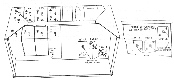
Figure 13 – Location of Trimmer Capacitors
36. CERAMIC CAPACITORS.|
Reference Number |
Old Description |
New Description |
|
32 |
Ceramic capacitor 138 mmf. +/- 1% |
Ceramic capacitor 134 mmf. +/- 1% |
|
33 |
Ceramic capacitor 110 mmf. +0 -5% |
Ceramic capacitor 106 mmf. +0 -5% |
|
40 |
Ceramic capacitor 74 mmf. +/- 2.5% |
Ceramic capacitor 72 mmf. +/- 2.5% |
|
43 |
Ceramic capacitor 62 mmf. +/- 3% |
Ceramic capacitor 60 mmf. +/- 3% |
|
48 |
Ceramic capacitor 22 mmf. +/- 5% |
Ceramic capacitor 20 mmf. +/- 5% |
|
49 |
Ceramic capacitor 20 mmf. +/- 5% |
Ceramic capacitor 18 mmf. +/- 5% |
|
50 |
Ceramic capacitor 20 mmf. +/- 1.5% |
Ceramic capacitor 1.5% |
|
NOTICE Connected for Iow impedance output |
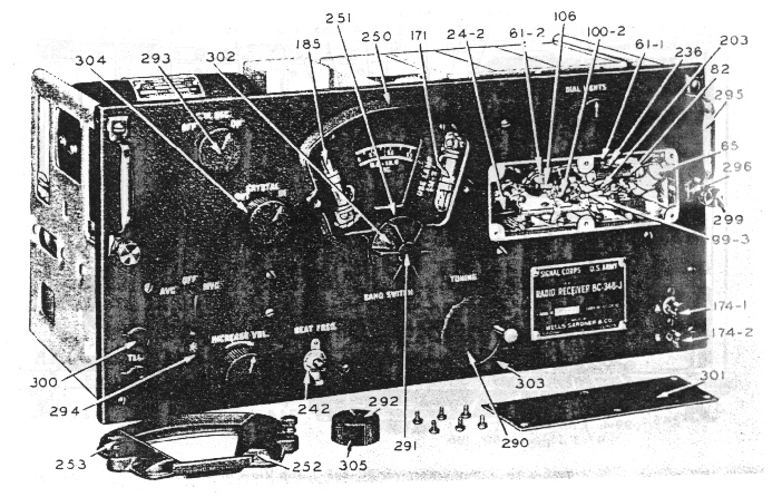
Figure 14 -- Radio Receiver BC-348-J, Front View
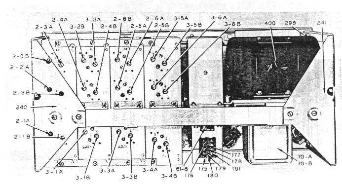
Figure 15 -- Radio Receiver BC-348-J, Rear View of Chassis
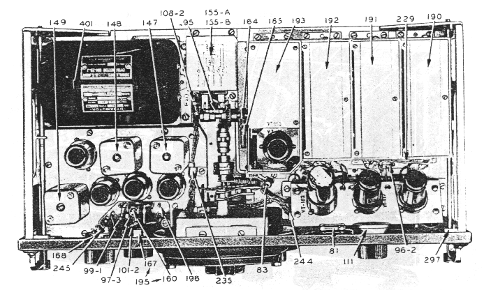
Figure 16 -- Radio Receiver BC-348-J, Top View of Chassis
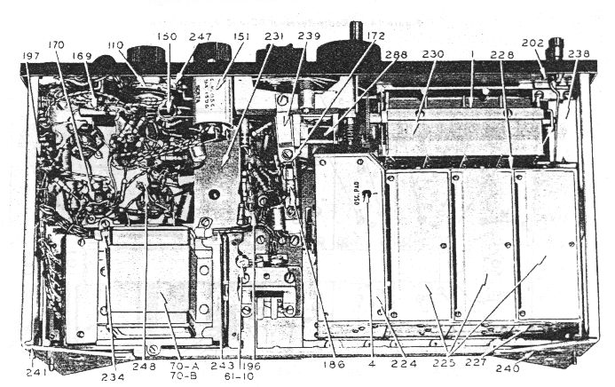
Figure 17 -- Radio Receiver BC-348-J, Bottom View of Chassis
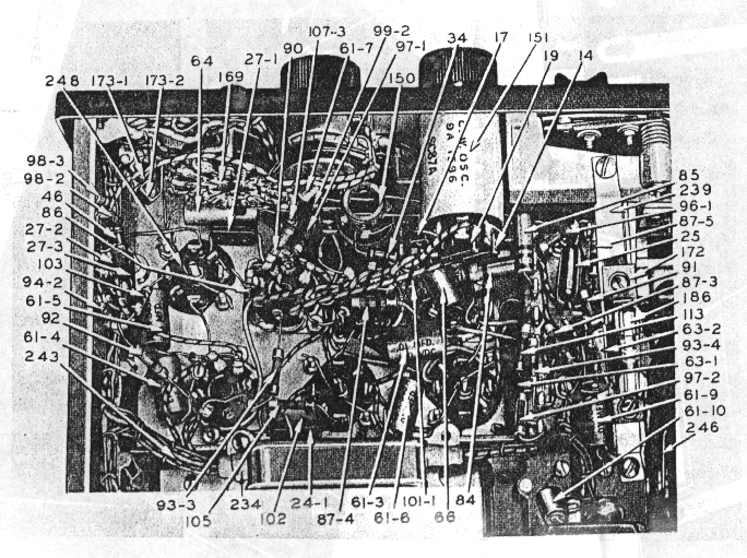
Figure 18 -- Radio Receiver BC-348-J, Partial Bottom View
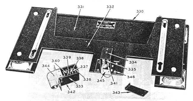
Figure 19 -- Mountings FT-154-J, FT-154-Q and FT-154-AA with Plug Assemblies, Rear View
Figure 20 -- Radio Receiver BC-348-J, Front View of Cabinet
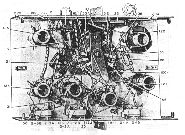
Figure 21 -- Antenna Unit
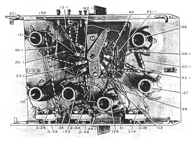
Figure 22 -- R.F. Unit
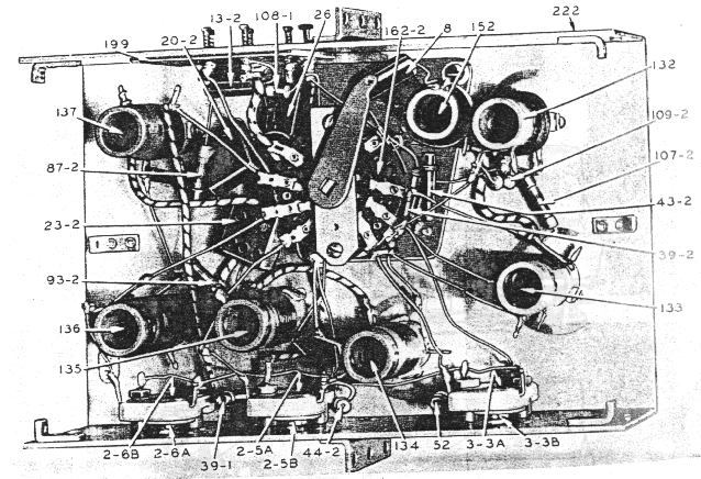
Figure 23 -- Detector Unit
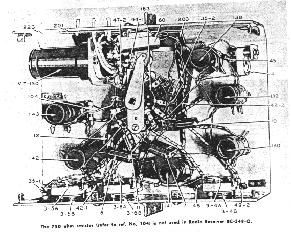
Figure 24 -- Oscillator Unit
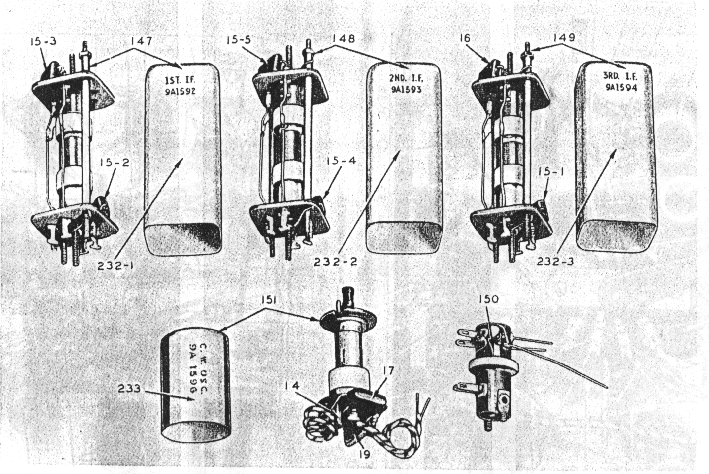
Figure 25 -- I-F C-W Oscillator and Crystal Coil Assemblies
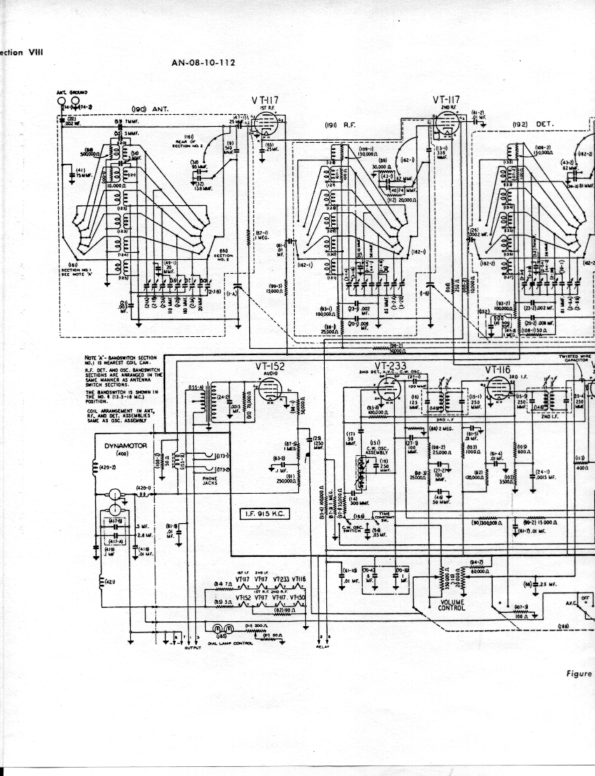
Figure 26-- Radio Receiver BC-348-J, Schematic Diagram (part 1)
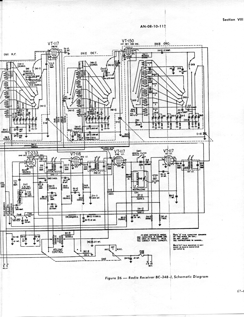
Figure 26-- Radio Receiver BC-348-J, Schematic Diagram (part 2)
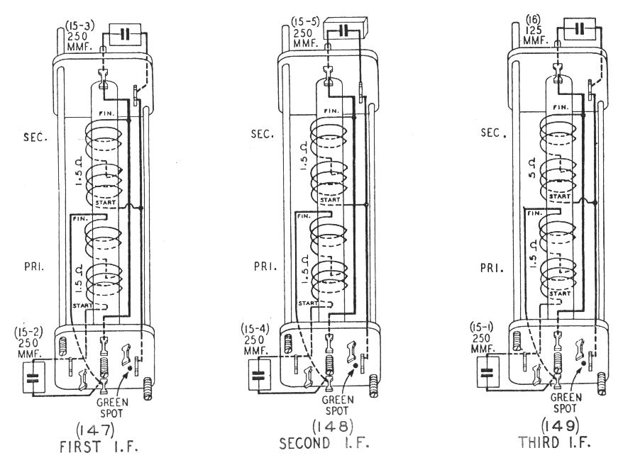
Figure 27-- I-F Transformers, Wiring Diagram
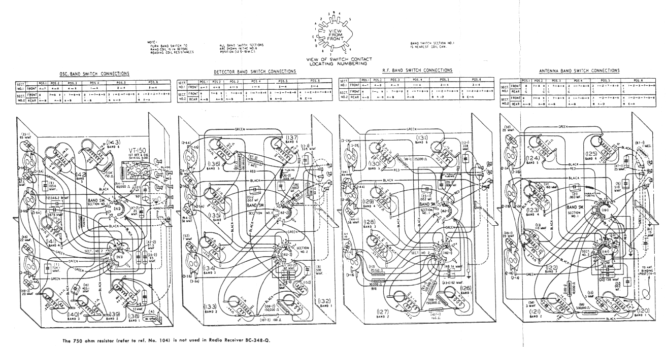
Figure 31-- Antenna, R.F., Detector and Oscillator Units, Wiring Diagram
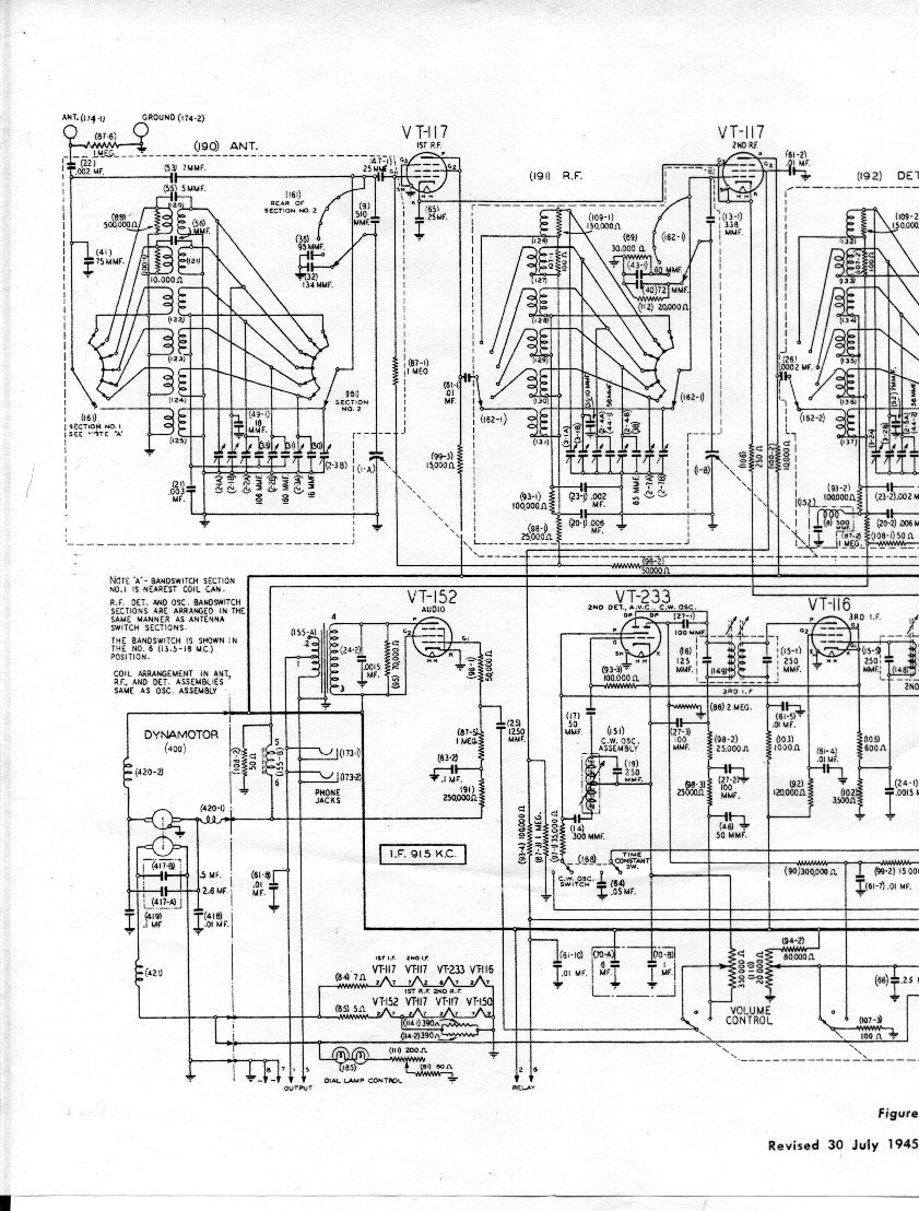
Figure 33-- Radio Receiver BC-348-Q, Schematic Diagram (part 1)
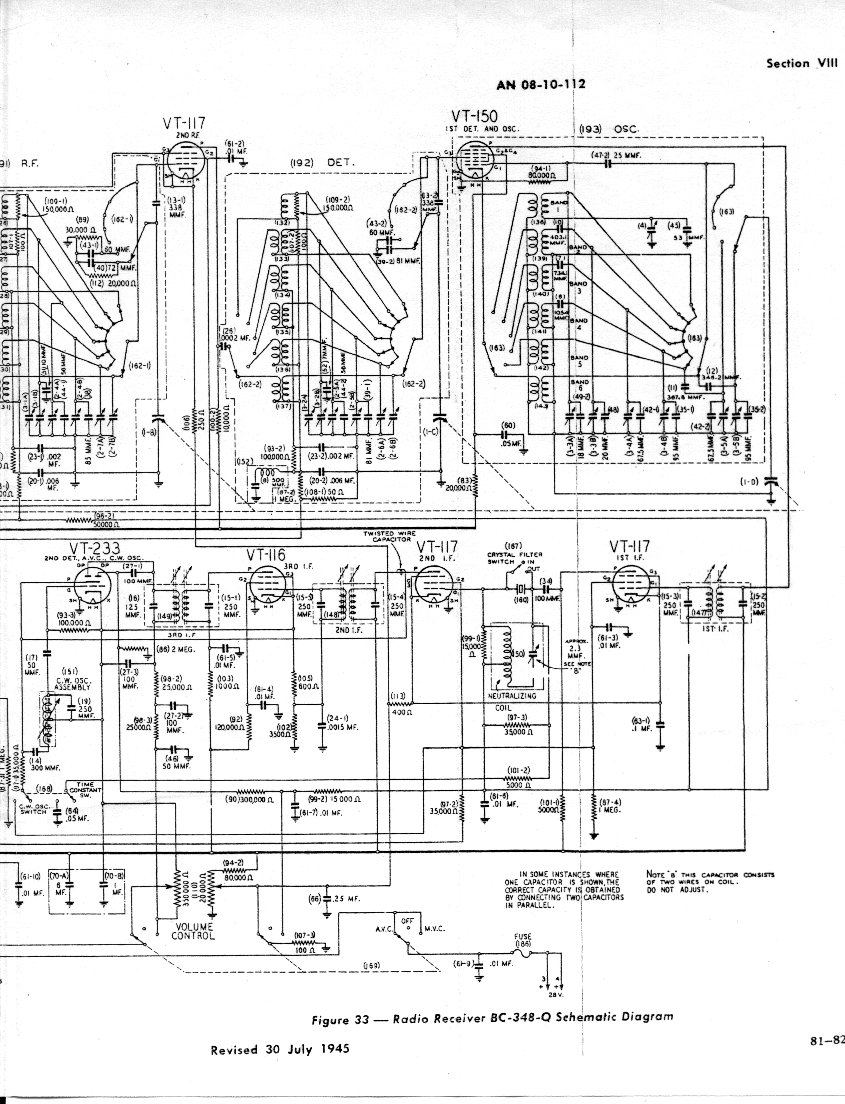
Figure 33-- Radio Receiver BC-348-Q, Schematic Diagram (part 2)
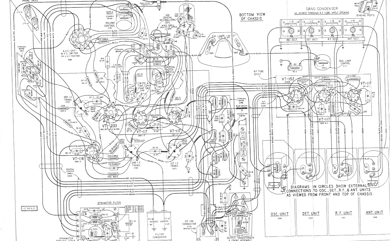
Figure 34-- Radio Receiver BC-348-Q, Wiring Diagram of Chassis